Hey there, let’s cut to the chase – if you work with PCBs (or even if you just dabble in the world of electronics manufacturing), you’ve probably heard the term “PCB assembly” a million times. But if someone drops “depanelization” in the same breath, do you know exactly what that means? I’m Jake, part of the team at our PCB assembly shop, and I’ve been in this game for 7 years – let’s break this down like we’re chatting over a coffee (no stuffy jargon, promise). PCB Assembly

First, let’s set the scene. Most of us don’t get single PCBs built, right? We order a bunch of identical tiny boards for phones, wearables, or even industrial sensors. Manufacturing single boards would be a nightmare for cost, time, and precision – so PCB fab guys make big, flexible panels that hold dozens (or hundreds) of the same PCB. Think of it like a cookie sheet covered in identical sugar cookies – the whole sheet goes into the oven, you bake all of them at once, then you separate each cookie later. That panel of PCBs? That’s your starting point for assembly.
Now, here’s where depanelization comes in. Once those panels come to us (the assembly team), we slap all the components on them – resistors, ICs, capacitors, even tiny surface-mount parts you can barely see. After we solder everything, we can’t send that big panel to the customer. They want individual, ready-to-use PCBs. So depanelization is simply the process of cutting that big panel apart into individual, finished PCBs after assembly.
Wait, hold up – it’s not just hacking at it with a utility knife. If you do that, you’ll chip solder pads, bend parts, or even crack the PCB itself. We’ve all seen that horror story: a customer gets their boards back, and half the pins are missing because someone sliced too hard. That’s why depanelization is super specific, and picking the wrong method kills both quality and yield.
Let’s talk about the main methods we use at our shop, because this isn’t one-size-fits-all. First, there’s v-scoring – that’s probably the most common, especially for flexible panels. If you look at the edges of a PCB panel, you’ll see thin, grooved V-shapes milled into the board material between each individual PCB. It’s like a pre-made line of weak points. For small, low-stakes boards, we use a v-score router or even a hydraulic press to snap them apart. It’s fast, cheap, and works great for most consumer electronics. But wait – if the V-score is too deep or too shallow, you get problems. Too deep, and you might crack the inner layers of the board. Too shallow, and you have burrs (those rough little edges) that can short out parts later. We check every panel’s v-score depth before we cut – rule of thumb is it should be about 1/2 to 2/3 the thickness of the PCB, not more.
Then there’s routing, for when v-scoring won’t cut it (pun intended). Routing uses a tiny, high-speed router bit – like the ones on a CNC machine, but way smaller – to carve a clean path between each PCB. This is our go-to for high-precision boards, especially if they’re complex, have tight tolerances, or are thick (like industrial control boards that need to hold up to a lot of stress). The cool thing about routing is you can customize the cut path to avoid any tricky spots, like test points or solder pads that are close to the edge. The downside? It’s a little slower and more expensive than v-scoring, because each board gets a unique cut path. But for customers building medical devices or aerospace parts? We’d never risk a snap that could misalign a tiny sensor, so routing is non-negotiable.
Oh, and let’s not forget breaking bars – wait, that’s another method for really small, super flexible boards. If you’ve got a panel of tiny boards for Bluetooth earbuds or wearables, sometimes we use a break bar: a rigid bar that lines up along the v-score line, and you apply even pressure to snap the board apart. It’s quick, and leaves super clean edges, but only works for really thin, flexible PCBs. We don’t use this for anything thicker than 1mm, because thicker boards just snap unevenly.
Now, here’s the part that trips up a lot of first-time customers: when do we do depanelization? A lot of people ask, “Why not do it before assembly?” Let me spell that out. If you take the panel apart first, each individual PCB is tiny, and surface-mount component placement becomes almost impossible. Those 0402 resistors (the size of a grain of sand) would bounce off a tiny board when we run the pick-and-place machine. Also, the panel gives us rigidity – when we’re soldering all the components, the panel doesn’t flex, so the solder joints stay even and consistent. Do it before, and you get a ton of misaligned parts and higher defect rates. So yeah, post-assembly is the only smart way to go.
But wait – we don’t just cut and ship. Part of our job as an assembly shop is to make sure depanelization doesn’t cause problems. We do post-depanelization inspection every single time. What are we checking for? Burrs that could scratch other parts, solder pad damage, cracks in the PCB substrate, or even leftover plastic shavings that could get stuck on the boards and cause shorts. For example, if we routed a board for a pacemaker sensor, we’re way more thorough than if we’re making a batch of toy PCBs. Quality isn’t optional here.
Let’s talk about some common mistakes we see customers make, too. One big one is not accounting for depanelization in their design. If you design a PCB with no space between the edges of adjacent boards, we can’t cut them apart without ruining the parts. Or if you place critical components right up to the edge of the PCB, the router bit (or v-score) might nick them. Another mistake is picking the wrong depanel method for the job. I once had a customer who ordered 1000 medical PCBs, and they insisted on v-scoring because it was cheaper. We tried to talk them out of it – their boards had high-precision antenna traces right on the edge – but they pushed it. The first batch came back with 8% defect rate from cracked traces. We re-did them with routing, and the defect rate dropped to 0.5%. Lesson learned: if you’re not sure which method is right, ask your assembly team. We’ve seen it all, and we can save you a lot of headache.
So why does this matter to you? If you’re a design engineer at a startup, a production manager at a mid-sized company, or even a hobbyist scaling up a prototype, depanelization isn’t a throwaway step – it’s part of the end product. A clean, defect-free depanel means your PCBs will work as intended, meet regulatory standards (especially for medical or aerospace), and save you from having to scrap a whole batch of boards.
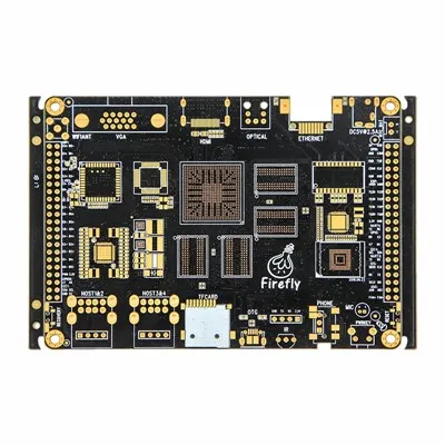
At our shop, we’ve been refining our depanelization process for years. We invest in both high-precision routing machines and v-score presses, so we can handle anything from tiny 0.5mm flexible boards to thick 5mm industrial control PCBs. We also work closely with our customers during the design phase, so we can tweak their panel layout to make depanelization easier and more reliable. No one wants to waste time or money on a step that should be seamless.
Quick Turn PCB Assembly If you’re working on a new project, or you’re tired of dealing with bad depanelization ruining your batches, hit us up for a consultation. We can walk you through the best depanel method for your specific needs, answer any questions you have, and make sure your PCBs get from panel to finished part without a single hiccup.
References
- Printed Circuit Board Association. (2022). Depanelization Best Practices for High-Volume Electronics Manufacturing. IPC-A-600 Revision F.
- Tummala, R. R. (2019). Fundamentals of Microelectronics Packaging. McGraw-Hill.
- Circuit Assembly Magazine. (2021). A Guide to Depanelization Methods and Quality Control.
- Electropaedia. (2020). PCB Panelization and Depanelization: Key Considerations for Yield and Reliability.
Huaswin Electronics Technology Co., Ltd.
With abundant experience, we are one of the most professional pcb assembly manufacturers and suppliers in China. Welcome to wholesale customized pcb assembly at competitive price from our factory. If you have any enquiry about pricelist, please feel free to email us.
Address: Building A2, Hao Hai Hong Industrial Park, No.3 Yu He Road, Gong He, Sha Jing, Bao An, Shenzhen
E-mail: sales@huaswin.com
WebSite: https://www.huaswin-pcba.com/
